Dual-nitride Quantum Wells Effects on Laser Diodes
Dual-nitride Quantum Wells Effects on Laser Diodes
Abstraction: This paper examines the public presentation of optical asymmetric dual-nitride quantum good focused, the sum of visible radiation in the dual quantum good structures with different structural parametric quantities were investigated. Vision charts utilize different mole fraction of aluminium in the barrier beds changes the breadth of the quantum good and barrier across the center in the scope of 1 to 5 nanometer is simulated. The consequences show an addition in the breadth of the quantum good and the rise in the center of the barrier to cut down the breadth of the visible radiation.
Keywords: quantum good, nitride, laser rectifying tube.
Order custom essay Dual-nitride Quantum Wells Effects on Laser Diodes with free plagiarism report
 450+ experts on 30 subjects
 Starting from 3 hours delivery
Introduction:
The semiconducting material quantum well optical masers have attracted many research workers. This tool is particularly widespread usage in devices such optical masers because of the highly low threshold currents, The narrow scope of the optical maser visible radiation and less dependent on temperature than normal, doing more and more industries are scrambling to optimise these devices is semiconducting material. The light one of the most basic features of a semiconducting material optical maser is to optimise the direct consequence of the external profile such as the efficiency and power end product. On the other manus, when the active bed construction are little plenty energy province in the conductivity set and quantal capacity and merely certain energy degrees are allowed. The thin active country is a great advantage and that is that the entire figure of bearers required to obtain a denseness of transparence in the active quantum good laser than conventional laser proportion of the thickness of the active country. [ 1 ]
Broadband spread stuffs and elements ( AlN, GaN, and InN ) associated with much success in optoelectronic devices, particularly in the present decennary have, Although these stuffs belong to the group, and ionic substances are polarized. There is a really big electric field in the way of growing of nitride stuffs for their piezoelectric consequence and self-generated polarisation. [ 2 ]
Working
In this paper the asymmetric double quantum good that the connexion is created, the undermentioned explains:
AluminumtenTabun1-xN /GaN / AltenTabun1-xN /GaN / AltenTabun1-xNitrogen
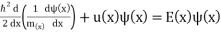
Fixed breadth of barrier and the breadth of the two Wellss will changed from 1nm to 5nm. It is deserving observing in this reappraisal due to the symmetricalness of the quantum Wellss of the effects of self-generated and piezoelectric Fieldss is neglected [ 3 ] . To cipher the first optical moving ridge map and the energy set is seeking to make, the Schrodinger equation for a atom in asymmetric quantum well is expressed as follows:
 ………… . ( 1 )
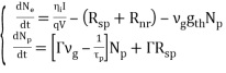
Where m( ten )is the effectual mass depends on the location of the well and barrier, U ( x ) is the profile represents the set construction. In work outing this equation finite difference method, the job with boundary conditions in a peculiar matrix becomes a value. Particular values of this matrix, the allowable energy systems and particular maps of the matrix, Particle wave map is the same [ 4 ] . A measure alteration from high to low degrees seen in Step 1 Angstrom energy degrees and beckon maps are accurate. To go on working, it is necessary to find the place of the Fermi degree by the degree by and large related to the injection of bearers and therefore a individual optical maser solution, the denseness of the bearers and so, degrees Dirac-like signifier of the Fermi distribution map achieved [ 5 ] . Song equations will be as follows:
 …………………… . ( 2 )
Where Ne the denseness of bearers, I current injection, ? bounds factor, ?ggroup speed equal to C/neff, gThursdaythreshold addition and as gThursday= ?I+ ?mwere as follows:
 ………………… ( 3 )
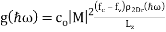
And Np the denseness of photons, Rsp self-generated emanation rate, Rnr non-radiation emanation rate, ?p photon life-time, which is equal to
 ………………… ( 4 )
Where degree Celsius is the vacuity light velocity, neff is the refractile index, L is the pit length, R1 and R2 are the pit mirrors coefficient of reflection, and ?i is the internal loss. The rate equations, numerically and by PCBF 4th with MATLAB, come closing quasi-Fermi degrees calculated [ 6 ] .
Given these physical parametric quantities can be achieved utilizing visible radiation that is expressed as follows:
 ………………… . ( 5 )
 ………………… . ( 6 )
 ………………… . ( 7 )
 ………………… . ( 8 )
Equation ( 8 ) built-in conductivity and valency sets overlap and some are less than one and really near to one. Harmonizing to equation ( 5 ) when the incident light moving ridge with involvement is positive and a photon, energy
 will be strengthened by the stuff. It can be shown that this inequality is tantamount to the term
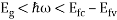 . The comparative separation of the Fermi degree must be larger than the set spread of the visible radiation in the stuff obtained. For high negatron bearer denseness can be made
 .
.
The Consequences
The construction consists of a barrier were studied type with AlGaN mole fraction x = 0.7, two Wellss of GaN with a thickness of 1nm. A barrier between the quantum Wellss of the AlGaN mole fraction x = 0.2 and breadth of 1nm and eventually a barrier is made of AlGaN fraction x = 0.7 as shown in fig. ( 1 and 2 ) .
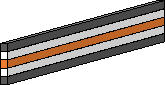
Figure 1: Schematic of the construction of the survey
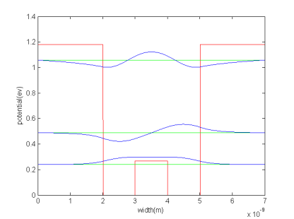
Figure 2: The moving ridge map and energy degrees for double asymmetric potency Wellss for negatrons.
In portion ( a ) can be fixed within the barrier and increase the breadth of the Wellss, the light lessenings as shown figure ( 3 and 4 ) . The cause of this diminution can be explained so that the breadth of the well additions, take part less in emanation and therefore the figure of photons produced by the reduced allowable passages. In portion ( B ) Wellss were fixed within 1nm and the breadth of the barrier will alter from 1nm to 5nm. Plug the center, similar to the alterations good, the moving ridge map and energy degrees and optical efficiency will cut down this consequence as shown in fig. ( 5 and 6 ) . In portion ( degree Celsius ) of the first good presuming changeless breadth and comprehensiveness of the barrier, with increasing breadth as the 2nd good as shown in fig. ( 7 and 8 ) , the visible radiation will be cut down.
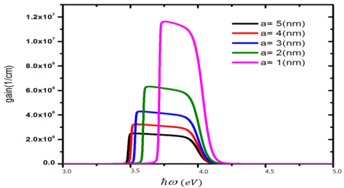
Figure 3: Optical addition in asymmetric dual quantum good nitride for assorted good width.
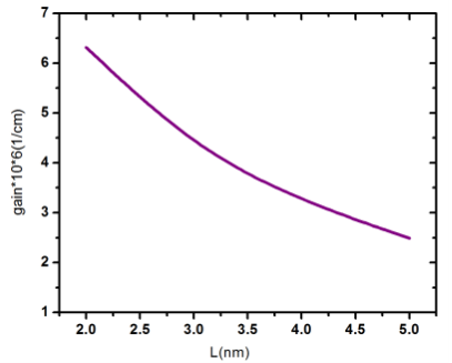
Figure 4: Change the visible radiation to alter the breadth of the asymmetric dual-nitride quantum Wellss.

Figure 5: Optical addition in asymmetric dual quantum good nitride for assorted mid-latitude blocking.
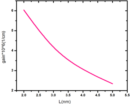
Figure 6: Change the visible radiation to alter the breadth of the barrier in asymmetric dual quantum good nitride.
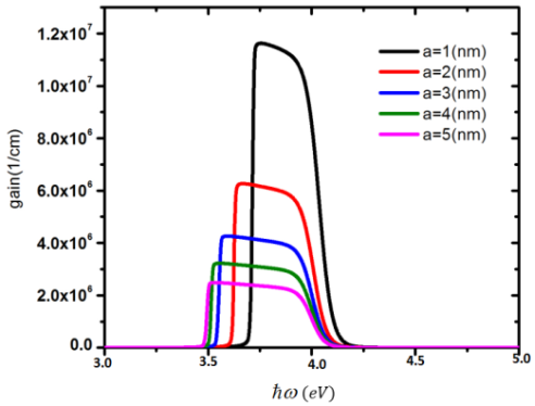
Figure 7: Optical addition in asymmetric dual quantum good nitride for alteration in one well.
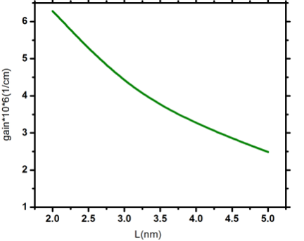
Figure 8: Change the visible radiation to alter the breadth of an asymmetric dual-nitride quantum Wellss.
Decision
This paper examines the asymmetric dual quantum good nitride laser visible radiation is focused. Calculations show that the impact on the type of optical maser is really high so that by increasing the breadth of the quantum good and increase the breadth of the barrier, reduced productiveness and increased breadth of the emanation spectrum.
Mentions:
[ 1 ] Peter, S. , Zory, J. , `` Quantum Well Lasers '' , Elsevier, 2012
[ 2 ] Berrah, S. , Abid, H. , Boukortt, A. , Sehil, M. , ``Band spread of three-dimensional AlN, GaN and InN compounds under force per unit area`` , Turk J Phys, 30, 513–518, 2006.
[ 3 ] Agrawal, G. , `` Fiber-optic Communication Systems '' , Wiley Interscience, 2000.
[ 4 ] LOEHR, J. , `` Physicss of Strained Quantum Well Lasers '' , Springer Science & A ; Business Media, LLC, 1998.
[ 5 ] Ivanov, P. S. , Lysak, V. V. , Sukhoivanov, I. A. , ``Advanced theoretical account for simulation of surface-emitting quantum-well optical masers`` , Int. J. Numer. Model, 14, 379-394, 2001.
[ 6 ] Suhara, T. , Semiconductor Laser Fundamentals, Marcel Dekker, Inc. , 2004
Cite this Page
Dual-nitride Quantum Wells Effects on Laser Diodes. (2018, Aug 02). Retrieved from https://phdessay.com/dual-nitride-quantum-wells-effects-on-laser-diodes/
Run a free check or have your essay done for you